APPLICATIONS
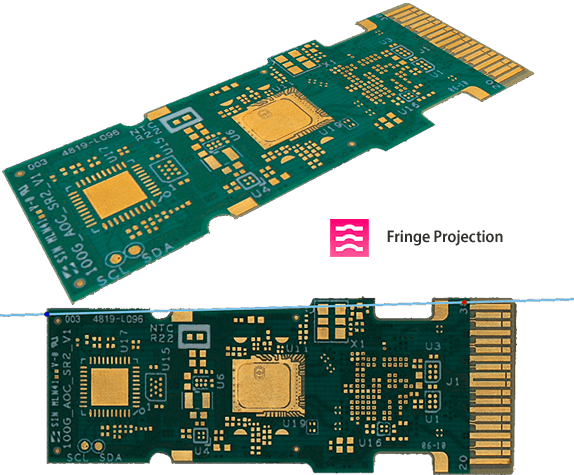
Manufacturing PCBs can vary greatly depending on the purpose and design of the board. Nevertheless, there are common elements that apply to all PCBs that are critical for their correct function. Sensofar has optimized its analysis software to copper circuits, vias, and pads.
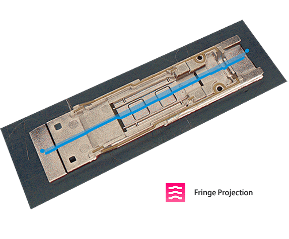
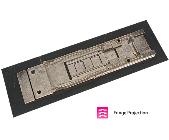
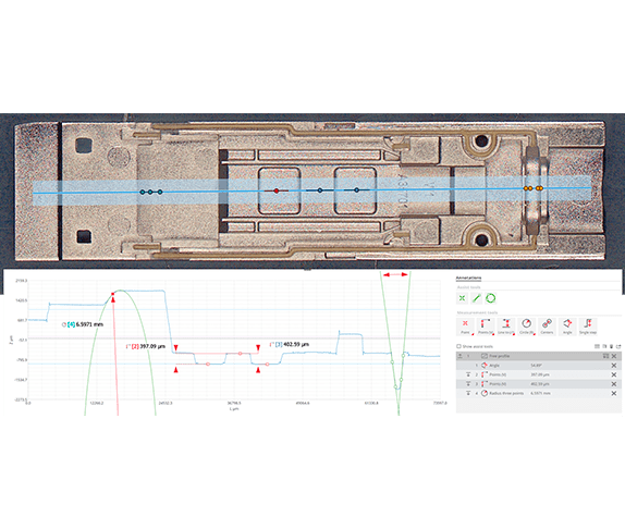
Metal component in PCB
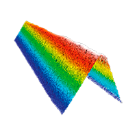
In here we have a metal component for an electrical appliance. Several critical dimensions are checked in every piece made, meaning SensoVIEW’s manual approach suits the characterization of this sample type.
PCB packaging
compatibility
After all the manufacturing process of a PCB, the flatness of the board is checked to ensure that the PCB fits well in its packaging. Flatness is characterized with the Sz parameter, calculated in SensoVIEW by default.
We can see where the highest and lowest points are located because SensoVIEW’s profiling options include the possibility to draw profiles with the highest and lowest points included.
Welding
opening pad
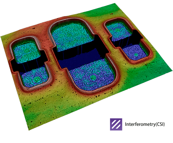
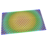
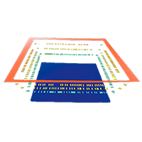
Knowing the most common disposition of pads, Sensofar has developed a specific plugin to recognize the individual pads or in any given pattern.
Copper trace
thickness
under dry film
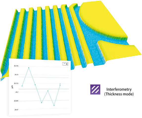
Interferometry and Confocal thickness are key technologies for this application. We can use both technologies to see which one images better through the layer, but also to verify and correct the results when the layer affects the measured height.
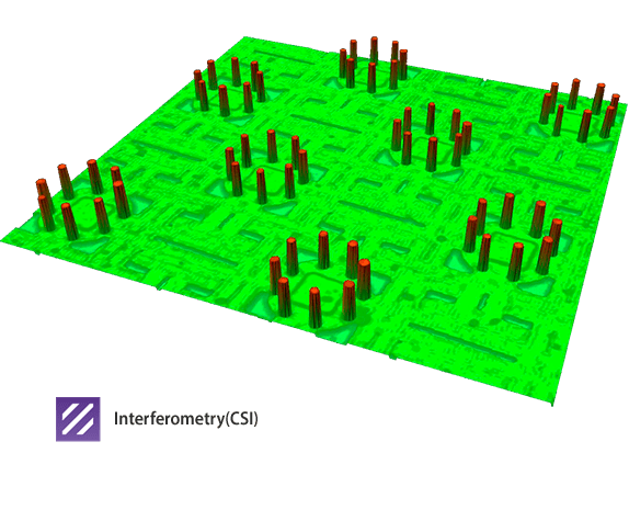
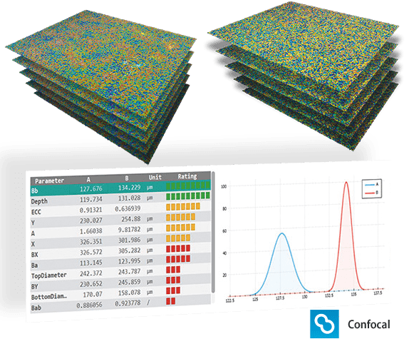
FTrace plugin automatically detects traces in different directions. All the plugins in SensoPRO have the possibility to see the tendency of values per each parameter.
Bump characterization
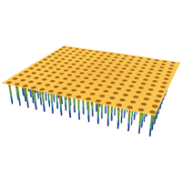
These structures are the base of the pins that the chip will have. Their position, height and diameter will determine the bump-pin union.
The Bump plugin can analyze up to 14.500 bumps.
Solder mask
welding
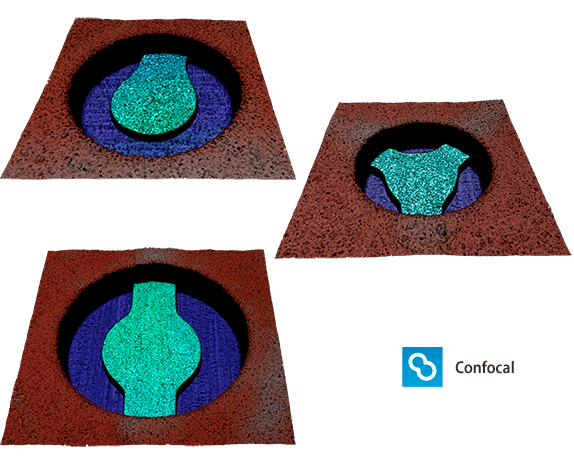
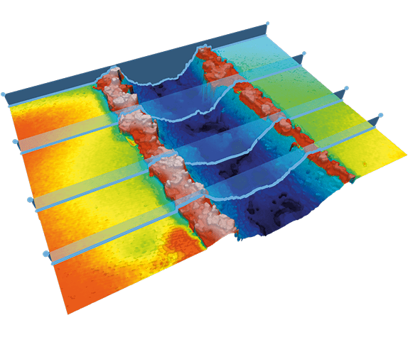
Solder Mask layers are usually applied to printed circuit boards (PCB) as protective layers. Openings for connections can have multiple connectors. The Solder mask plugin can easily recognize the different configurations and analyze the key parameters.
Laser groove
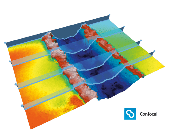
Laser cutting is one of the main front-end processes in the semiconductors field. In the case of PCBs, it is used for fabricating bias and channels of communication that are characterized (barbs, depth, etc.).
Grove profile plugin has been developed to analyze different structures generated with laser methodology.
Copper wire adhesion
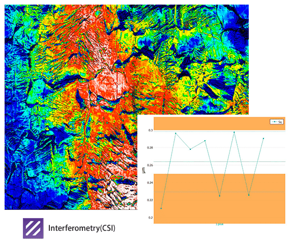
The surface finish of materials impacts the material’s behavior. In this case, the interesting property is the adhesion of copper with a conductive material used in the welding process.
Understanding which roughness parameter differentiates two sets of samples with different adhesion can help the user to correlate specific roughness parameters with adhesion and this can be done with the Surface texture plugin of SensoPRO.
Gold foil
High-end microelectronics use a gold foil since this metal has a better performance than other materials used in the application. Defects on the surface or roughness values different than the optimal can severely affect the top layers.
With the powerful Surface texture plugin, it can apply tolerancing to know which parts do not comply.


