Dual-technology optical sensor head for 3D surface shape measurements on the micro and nano-scales

Holder of several patents in the field of Optical Surface Metrology.
Technical committee member of the ISO 25178.
Co-founder of Sensofar in 2001.
Roger has been working since 1997 to the present at the Centre for Sensors, Instruments and Systems Development (CD6) as optical engineer researcher. From 2005 to the present is part of the TG WG16 committee of the ISO25178 standard which is applied in the field of equipment developed in Sensofar. Currently he holds the position of President and CTO at Sensofar Tech SL.


Dual-technology optical sensor head for 3D surface shape measurements on the micro and nano-scales publication
Roger Artigas 1, Ferran Laguarta 1, Cristina Cadevall 1
1 Center for Sensors, Instruments and Systems Development (CD6), Universitat Politècnica de Catalunya (UPC) Rambla Sant Nebridi, 10, E-08222 Terrassa, Spain.
January 2004, Proceedings of SPIE – The International Society for Optical Engineering 5457:166-174
Conference: Conference on Optical Metrology in Production EngineeringVolume: 5457
Abstract
New material applications and novel manufacturing processes are driving a systematic rise in market demands concerning surface inspection methods and the performance of non-contact profilers. However, analysis of the specifications and application notes of commercial optical profilers shows that no single system is able to offer all the features a general purpose user would like simultaneously. Whereas white light interferometers can achieve very fast measurements on the micro and nano-scale without any range limitation, they can not easily deal with steep smooth surfaces or structured samples containing dissimilar materials. PSI techniques allow the user to perform shape and texture measurements even below the 0.1 nm scale, but they have an extremely short measurement range. Imaging confocal profilers overcome most of these difficulties. They provide the best lateral resolution achievable with an optical profiler, but they have a resolution limit, which is dependent on the NA and cannot achieve the 0.1 nm vertical resolution. In this paper we introduce a new dual-technology (confocal & interferometer) illumination hardware setup. With this new sensor head it is possible to choose between standard microscope imaging, confocal imaging, confocal profiling, PSI and white light interferometry, by simply placing the right objective on the revolving nosepiece.
1. Introduction
In recent years, there has been considerable competition among the manufacturers of interferometers and confocal imaging profilers in order to conquer the non-contact surface metrology market. Both systems are capable of accurately and reliably measuring surface topographies on the scale of millimeters to nanometers. However, the measurement principles involved in these techniques are very different and, as a result, the capabilities of interferometers and confocal profilers seem to be more complementary than coincident.
In this paper we will focus on a novel dual-technology (confocal & interferometer) sensor head for 3D surface shape measurements on the micro and nano-scales. This concept is a real breakthrough in non-contact optical profiling.
In Section 2 we review and compare the specifications of the different image-based profiling technologies: Confocal Imaging Profilers, Phase Shift Interferometers (PSI) and White light Vertical Scanning Interferometers (VSI). The analysis of the specifications of the various systems shows that none of the commercial optical profilers is able to offer all the features that a general-purpose user might require. Whereas white light interferometers can perform very fast measurements on the micro and nano-scale without any range limitation, they cannot easily deal with steep, smooth surfaces or stratified samples that contain dissimilar materials. PSI techniques allow the user to perform shape and texture measurements even below the 0.1 nm scale, but they have an extremely short measurement range, and are subject to the limitations inherent to all interferometers. Imaging confocal profilers overcome most of these difficulties. They provide the best lateral resolution that can be achieved with an optical profiler. However, vertical resolution, which is dependent on the NA, is still limited and the 0.1 nm figure cannot be achieved.
In Section 3 we introduce the new dual-technology illumination hardware. This sensor has been developed by UPC-CD6 and Sensofar using microdisplay technology without any moving part inside the measuring head. With this system it is possible to choose between standard microscope imaging, confocal imaging, confocal profiling, PSI and VSI. The user simply has to choose the right objective and select the appropriate acquisition and data processing algorithms. Moreover, the compact design of the sensor head breaks the traditional microscope appearance of most of optical profilers and makes it possible to build up many different configurations; from the simple stand set-up for R&D and quality inspection laboratory to the most complete and sophisticated arrangements for on-line process control.
In Section 4 we show several measurements performed with the new optical profiler. The advantages of confocal technology in combination with the interference techniques provide a unique wide spectrum of applications. The examples show that the dual-technology sensor head is suitable for repeatable and accurate profiling of very flat and smooth surfaces with shape features on the nanometer scale, but also for the measurement of very rough surfaces, high aspect ratio features, steep smooth surfaces and steeply sloping samples. Step height measurements can also be made using confocal technology in structured or stratified samples containing dissimilar materials.
Finally, some conclusions related to the implementation and the modularity of such an optical imaging profiler are drawn.
2. Technology and specifications review
Confocal profilers have been developed to measure the surface height of surfaces ranging from smooth to very rough1-4. The sample is scanned vertically in steps so that every point on the surface passes through the focus. The height of the surface at each pixel location is found by detecting the peak of the narrow axial response. Because only one or a few points of the surface are illuminated at the same time, in-plane raster scanning is also required in order to build the axial response (i.e. the confocal image) at each vertical step.
In an interferometer, a light beam passes through a beam splitter, which directs the light to both the surface of the sample and a built-in reference mirror. The light reflected from these surfaces recombines and a fringe interference pattern is formed.
Phase Shift Interferometers (PSI) have been developed to measure the surface height of very smooth and continuous surfaces with sub-nanometer resolution. The sample, which must be in focus, is scanned vertically in a few steps, which are a very precise fraction of the wavelength. The profiling algorithms produce a phase map of the surface, which is converted to the corresponding height map by means of a suitable unwrapping procedure 5-7 .
White-light vertical scanning interferometers (VSI) have been developed to measure the surface height of smooth to moderately rough surfaces. Maximum fringe contrast occurs at the best focus position for each point on the surface of the sample. The sample is scanned vertically in steps so that every point on the surface passes through the focus. The height of the surface at each pixel location is found by detecting the peak of the narrow fringe envelopes 8-9 .
2.2 SPECIFICATIONS REVIEW
Concerning the microscope objectives available today, confocal profilers offer a very broad range of magnifications (from 5X to 200X) and numerical apertures (from 0.15 NA to 0.95 NA). Super long working distance objectives (from 20X to 100X SLWD) can also be used to measure high aspect ratio features, large steps and steeply sloping samples. In PSI and VSI interferometers a range of magnifications (from 1.5X to 50X) and numerical apertures (from 0.02 NA to 0.42 NA) are available. Magnifications higher than 50X can be obtained using Linnik objectives, but they are extremely expensive and unpractical.
The magnification of the objective used defines the field of view that can be measured on the surface of the sample. To overcome this limitation on the lateral range, most of imaging profilers can also measure extended topographies beyond a single field of view by acquiring and stitching several contiguous measurements.
As to lateral resolution, because of the illumination-detection setup, confocal technology provides the highest lateral resolution achievable by an optical profiler (close to 0.3 µm for 0.95 NA and wavelength of 500 nm). This makes it possible to reduce the spatial sampling down to 0.10 µm, which is ideal for critical dimensions measurements.
Vertical measurement using confocal and VSI technologies has intrinsically unlimited measurement ranges. In practice, however, VSI ranges are limited to 1mm. PSI technology has a vertical measurement range limited by the coherence length of the light source (i.e. just a few micrometers when standard bulb light sources and interference filters are used).
Concerning the vertical resolution and repeatability, in confocal profiling the axial response becomes broader as the NA decreases. Thus, resolution and repeatability are dependent on the objective used (1 nm repeatability can only be achieved with the highest available NA). Conversely, PSI & VSI profiling provide the same vertical resolution and repeatability for all NA (1 nm for VSI and 0.1 nm for PSI). Very low magnifications can be employed to measure large fields of view with the same height resolution. Independently of the profiling technology, closed-loop z-scan stages are always necessary in order to achieve the accuracy that provides calibration to traceable standards.
The maximum slope that can be profiled on a smooth surface is a key feature. Because of the high NA (0.95) of the objectives that can be used, confocal profilers are able to measure smooth surfaces with extremely steep local slopes (up to 70º). Interferometers can not reach these figures because of: (i) the limitations in the NA of the available objectives, and (ii) the limitations of the CCD arrays to adequately sample the interference fringes that become closer and closer together as the local slope of the surface is increased.
Unlike interferometers, confocal profilers can easily deal with flatness assessment and step height measurements in structured or stratified samples containing dissimilar materials 10.
Finally, as for the total measurement time, confocal profilers and interferometers are very similar. Whereas PSI and VSI techniques are extremely fast in the acquisition, they require more time to focus and level the samples. On the other hand, using the confocal technique it is very easy and fast to focus the surface and it is not necessary to level the sample, but acquisition is slower than with the interferometers. In the present, very fast acquisition rates (up to 100 µm/s) are available in commercial profilers, but these figures can only be achieved at the expense of a significant loss in vertical resolution.
3. Dual-technology illumination setup
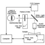
The basic setup of the illumination hardware is shown in Fig. 1a. The picture of the first prototype of the dual-technology sensor head, which has been developed by UPC-CD6 and Sensofar, is also shown in Fig. 1b. The light source is a high power LED, which is emitting at a peak wavelength of 480 nm with a lambertian emission pattern. The light beam coming from the LED is collimated before reaching a polarizing beam splitter cube (PBS). The resulting polarized beam strikes the ferroelectric liquid-crystal-on silicon (F-LCOS) microdisplay, which is placed on the field diaphragm position of the optical epi-illuminator setup. The F-LCOS is the key active device of the sensor head and the information transferred to the microdisplay will be imaged on the surface of the sample by the f/100mm field lens and a CFI60 infinity-corrected microscope objective. In this standard episcopic arrangement the surface of the illuminated sample will be also imaged on the CCD array.
When a white image (i.e. full-on state for all pixels of the LCOS) is displayed, the sample is illuminated in the whole field of view as in a standard microscope. Conventional microscope objectives will provide standard microscope imaging, whereas interference objectives will provide interference imaging.

In order to obtain confocal images a binary pattern is displayed in the LCOS and imaged onto the surface of the sample. The optical setup provides the required matching between pixels of the LCOS and pixels of the CCD array, which in turn behave as confocal apertures 2 . The axial response at each pixel position is calculated from the CCD frames using the appropriate algorithms 3,4 . Because only one or a few points of the surface are illuminated at the same time, in-plane raster scanning is necessary to build the axial response (i.e. the confocal image) at all pixel locations. In order to carry out the raster scan, a sequence of binary patterns is displayed in the LCOS until the complete field of view has been completely filled. As a result, confocal imaging is slower in comparison with standard or interference imaging because a sequence of CCD frames must be acquired to build one single confocal image.

As can be seen in Fig 1b, the complete epi-illuminator and the revolving nosepiece with the objectives are mounted on a vertical motor-driven linear stage. This allows the sensor head to scan the sample vertically in steps so that every point on the surface passes through the focus. The height of the surface at each pixel location is found by using the profiling technologies discussed in Section 2.1. The user simply has to choose the right objective and select the appropriate acquisition and data processing algorithms (confocal, PSI and VSI).
Moreover, the compact design of the sensor head breaks the trend in traditional microscope appearance for most optical profilers and makes many different configurations possible. Anything from the simple stand set-up for R&D and quality inspection laboratories, which is shown in Fig.2a, to the most complete and sophisticated arrangements for on-line process control, such as the robot-driven setup shown in Fig 2b, are now possible.
4. Measurements and applications
As stated above, the advantages of confocal technology in combination with the interference techniques provide a uniquely wide spectrum of applications. In this section we will show different applications with the aim of revealing the limits of the different techniques and, at the same time, to demonstrate that they can be complementary solutions in order to obtain the requested shape data for each sample.
Figures 3 and 4 show the results obtained in very smooth surfaces with nanometric features like a 50 nm step or a 90 nm dent. In this kind of samples, PSI is the right solution in order to overcome the limitation of VSI and confocal techniques to achieve resolution and repeatability figures on the sub-nanometric scale. Figures 5 and 6 show two smooth samples with very steep surfaces, in which confocal is the only applicable technique. Fig. 7 shows a confocal measurement of a structured sample containing three layers of dissimilar materials on a silicon substrate. Confocal results are coincident within 1% with contact stylus measurements, whereas VSI results show step height errors close to 10%. Finally, Fig. 8 shows very good measurements obtained on a MEM device with both, VSI and confocal techniques. However, because of the better lateral resolution, confocal technique provides better results in the measurement of the finest lateral features.


5. Conclusions
A new dual-technology (confocal & interferometer) illumination hardware setup has been developed. This sensor configuration provides the user with all the available imaging options (standard microscope, confocal and interferometry), as well as the highest resolution surface profiling techniques (confocal, PSI and VSI), by simply placing the right objective on the revolving nosepiece and selecting the appropriate acquisition and data processing algorithm. The advantages of confocal technology in combination with interference techniques provide a unique wide spectrum of applications. This means a real breakthrough in non-contact optical profiling on the micro and nano-scales.
Acknowledgements
This research was supported by the Ministerio de Ciencia y Tecnología, Spain. The project (Ref. DPI2002-01018) was partially financed by the EU-FEDER program. The authors would like to thank Dr. Andrei Skhel from the University of California, Irvine for supplying the MEMs samples used in Fig. 8.
References
[1] T. Wilson, Confocal microscopy, ed. Academic London, 1990
[2] F. Laguarta, I. Al-Khatib, and R. Artigas, Laser profiler based on the depth from focus principle, J. Opt. Vol. 29, pp. 236-240, 1998.
[3] F. Laguarta, R. Artigas, A. Pintó, and I. Al-Khatib, Micromeasurements on smooth surfaces with a new confocal optical profiler, Three dimensional imaging, optical metrology and inspection IV, SPIE Vol. 3520, pp. 149-160, (1998).
[4] R. Artigas, A. Pintó, and F. Laguarta, Three-dimensional micromeasurements on smooth and rough surfaces with a new confocal optical profiler, Optical Measurement Systems for Industrial Inspection, M Kujawinska and W. Osten ed., SPIE Vol. 3824, pp 93-104, 1999.
[5] J. E. Greivenkamp and J.H. Brunig, Phase shifting interferometers, Optical Shop Testing, D. Malacara, ed. Wiley, New York, 1992.
[6] J. Schmit and K. Creath, Extended averaging technique for derivation of error-compensating algorithms in phase shifting interferometry, Applied Optics, 34, pp. 3610-3619, 1995.
[7] D. Ghiglia and M.D. Pritt, Two-Dimensional Phase Unwrapping; Theory, Algorithms and Software, ed. John Wiley & Sons, 1998.
[8] M. Park and S. Kim, Direct quadratic polynomial fitting for fringe peak detection of white light scanning interferometry, Optical Engineering, Vol. 39, pp. 952-959, 2000.
[9] K.G. Larkin, Effective nonlinear algorithm for envelope detection in white light interferometry, J. Opt. Soc. Am. A13, pp. 832-843, 1996.
[10] C. Cadevall, R. Artigas, and F. Laguarta, Development of confocal-based techniques for shape measurements on structured surfaces containing dissimilar materials, SPIE Vol. 5144, pp. 206-217, 2003.