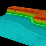
Wafer groove single line
PCB | SEMICONDUCTOR
This plugin characterizes in detail the first cut of the dicing process. To do so, it measures multiple dimensions of dicing traces made with lasers. Wafer Groove Single Line will detect one trace within the topography.


Wafer groove two lines
PCB | SEMICONDUCTOR
This plugin characterizes in detail the first cut of the dicing process. To do so, it measures multiple dimensions of dicing traces made with lasers. Wafer Groove Two Lines will detect two traces within the topography.


Wafer groove single line far
PCB | SEMICONDUCTOR
This plugin characterizes in detail the first cut of the dicing process. To do so, it measures multiple dimensions of dicing traces made with lasers. Wafer Groove Single Line will detect one trace within the topography.


Wafer groove two lines far
PCB | SEMICONDUCTOR
This plugin is used in the semiconductor manufacturing process to analyze three cuts made during dicing. It can calculate parameters from six trace lines to improve the manufacturing process. Integrators can include it with other plugins like Wafer Groove Single Line and Wafer Groove Two Lines to automate the cut analysis, reducing manual intervention and making the process more efficient.


Also, these four plugins bring an exciting display of detection. Find in the following graph a cross-section of the topography in which the points considered for the calculations are shown: