Start typing and press Enter to search

This website does not support Internet Explorer. For a correct visualization we recommend to use Microsoft Edge or Google Chrome.

CONSUMER ELECTRONICS

The consumer electronics market includes Semiconductors, Printed Circuit Boards (PCB’s) and Display industries, among others. Sensofar has become a true money saving tool in many applications given its speed and versatility.

  Measurement of critical dimensions of Wafer Level Chip Scale Packaging and photomasks.
  Chip edge measurements.
  Radius surface.
 
Roughness measurements on e.g., Copper.
 
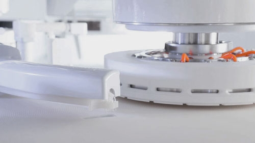
Wear characterization of polishing pads, dicing blades and grinding wheels.
  Solar Cell surface texture measurements.
  Probe depth measurements.
 
Automatic detection and analyses of holes, traces, trenches, step heights and bumps.
 
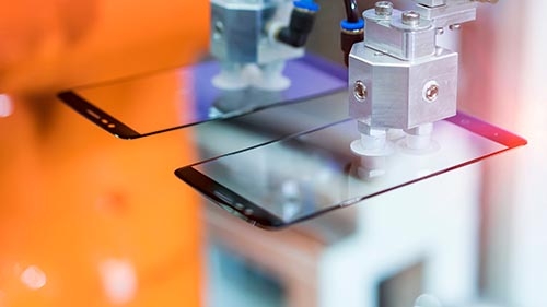
Nanometric measurement of defects on glass boards.
 
Thickness, Profile and roughness measurements of thin and thick optical films.

Applications

cmp
CMP
display
DISPLAY
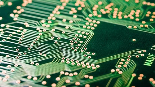
pcb_printed_circuit_board
PCB
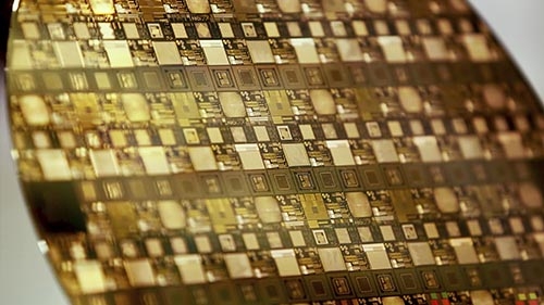
Silicon wafer
SEMICONDUCTORS
Fantasy circuit board.  3d illustration
SMT
conversation-icon_medium300x183

Get answers to your questions!
Connect with an expert

Just write us an email or search for
a direct contact near you.

conversation-icon_medium

Get answers to your questions!
Connect with an expert

Just write us an email or search for
a direct contact near you.

Webinar

Webinar precision 3d metrology semiconductor mfg

Precision 3D metrology for semiconductor manufacturing

In this 3D precision metrology semiconductor webinar, you’ll learn about wafer-level testing to final device verification.

In this 3D precision metrology semiconductor webinar, you’ll learn about wafer-level testing to final device verification.

Related publications Show all >