Characterizing the temperature-induced evolution of the shape and texture of a silicon wafer

Robert joined Linkam’s Sales and Marketing team in 2019 and has expertise in a range of scientific techniques for temperature, environmental and mechanical sample characterisation. He is responsible for Linkam’s scientific articles and marketing materials. Robert obtained his PhD in Soft Materials from the University of Surrey and has worked at ESPCI Paris and Wuhan University of Technology on projects including thin film analysis, chemical synthesis, and solar cell characterisation.

With extensive experience in optical 3D metrology, David works closely with customers and internal engineering teams to understand real-world measurement needs involving surface topography and dimensional inspection. Through this collaboration, he helps translate Sensofar’s metrology expertise into practical measurement strategies that enable engineers and researchers to gain reliable insight from their measurements and succeed in a wide range of industrial and research applications worldwide.

Using Linkam’s precision temperature control chamber with Sensofar’s Linnik objective lens eliminates these problems and allows accurate measurement of 3D topographic profiles of nanoscale materials
In this case study, Linkam and Sensofar Metrology demonstrate their collaboration in producing an experimental setup for temperature-controlled optical profilometry experiments. This has historically been a difficult procedure due to imaging issues caused by spherical aberrations. Using Linkam’s precision temperature control chamber with Sensofar’s Linnik objective lens eliminates these problems and allows accurate measurement of 3D topographic profiles of nanoscale materials. Here, we observe the changes in the topography of silicon wafers as they evolve with temperatures from 20°C up to 380°C.
Rapid Thermal Processing (RTP) is an important step in the manufacturing process of silicon wafers, in which the wafer is rapidly heated to high temperatures for a short period of time, then slowly cooled in a controlled manner, in order to impart the desired semiconducting properties to the wafer. However, RTP causes thermal stress which leads to other problems in photolithography that may affect the performance of the device, such as breakage due to thermal shock or dislocation of the molecular lattice. Understanding the behavior of a wafer under these conditions can help optimize the process, improving semiconductor properties and wafer durability.
A key method of evaluating the effects of temperature change during wafer manufacturing is to measure the surface roughness of the wafer as a function of temperature. To do this, the surface roughness is observed by an interferometry technique in conjunction with using a thermal chamber, allowing the temperature to be raised precisely to values similar to those during the manufacturing process while observing the sample through microscopy.

There are several factors that introduce some complexity in obtaining these interferometric measurements. Firstly, in order to visualize the sample and obtain the data while accurately controlling the temperature in the chamber, it is necessary to make observations through the chamber’s optical window. This window is 0.5mm in thickness, but in some cases, it can be as much as 1mm, depending on the degree of thermal insulation required. This window, being of a different refractive index to air, would introduce optical aberrations and misalignments that, when analyzing silicon wafers, should be corrected in order to obtain reliable data. Furthermore, when the temperature inside the chamber is increased, heat is emitted to the exterior through the observation window, and this is not ideal for optical microscopy. In the air close to that window, the temperature can reach 60 degrees Celsius, which can lead to deformation of the objective lens, introducing aberrations.
In order to address the experimental issues of interferometry at varying temperatures, a Linnik interferometer can be used. The Linnik interferometer introduces the use of measurement optics within the reference arm of a classic interferometer. This allows for compensation and correction of the effect of the optical window such as chromatic dispersion and optical aberrations, enabling work with brightfield objectives that have a greater working distance than traditional interferometric objectives.
In this work, we study the effect of the RTP process on the silicon wafers while accounting for optical aberrations brought about by temperature changes. Two different samples were used, corresponding to different chip designs from silicon wafers. Sample A was 2.8mm x 1mm in size, whereas Sample B was 3.0mm by 2.35mm. Silicon wafers have typical surface roughness values on the sub-micron scale, so the ideal optical technology for this application is Coherence Scanning Interferometry (CSI, ISO 25178, part 604). CSI offers only 1 nm of system noise, regardless of the magnification of the lens being used.
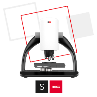
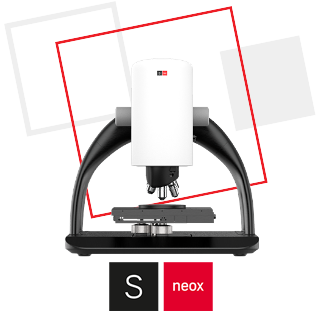
For the design and construction of the Linnik objective, two Nikon 10x EPI objectives (Nikon, MUE12100) with 17.5 mm working distance were used. The same configuration is available with 10xSLWD objectives (Nikon, MUE31100), providing a 37 mm working distance. This makes the thermal emissions from the camera almost imperceptible to the lens and will not affect or damage the measurement quality. The Linnik objective was mounted on the 3D optical profilometer (Sensofar, S neox), which combines 4 optical technologies in the same sensor head: Confocal, CSI, PSI and focus variation. These techniques are covered in ISO 25178.
The temperature is controlled using a Linkam LTS420 chamber and the T96 temperature controller, which allows the temperature to be ramped and controlled between -195° and 420°C to a precision of 0.01°C, while the sample roughness is observed through the chamber window. The chamber also allows control of the pressure and humidity, but this has not been investigated in this study.


The wafer sample was placed in the Linkam chamber under the S neox optical profiler with the Linnik configuration. The acquisition routine consisted of ramping the temperature from 30°C to 380°C in 50°C steps, taking 8 topographic measurements of the sample at each step. This procedure was repeated for three samples.

Using SensoMAP software, the results were visualized and analyzed by creating a template and applying it to all samples. The template allows the extraction of 3 profiles in each topography (horizontal, diagonal, and vertical) and representation in the same plot, and furthermore builds a sequence of the topographies to export it as a video and represent it in a 4D plot.
Two topographic images of the same sample were imaged using the above methodology and are shown in Figure 5 as two-dimensional height maps. The three solid lines represent the three different profiles (horizontal, vertical and diagonal) extracted for each topography. The profiles in each direction are shown in Figure 6, where we can see the evolution for the different temperatures at which the sample was taken. The images show that when heating the sample, its topography changes.


The data can be plotted in 3D topographic image as shown in Figure 7. By stacking the 3D images as a function of temperature, creating a “4D plot”, showing the topographical changes at different temperatures using the same height color scale, showing how the samples bend as temperature changes. It is clear that the higher the temperature, the greater the bending experienced by the samples.

To quantify the bow of the samples, two different parameters were used. The first is Sz, which is the surface roughness parameter for the maximum height of a surface according to ISO 25178. The second is Wz, corresponding to the counterpart of Sz in profile analysis (ISO 4287). Both Sz and Wz were obtained after applying an S-filter to the surface (or profile) with a 0.8mm cut-off. In this way, only the longer spatial wavelengths remain on the surface, getting rid of roughness and only leaving waviness for bow analysis.
The resulting parameters for samples A and B are depicted in Figure 9. For sample A, an almost-linear relationship is observed between bow and temperature up to 180ºC, which stabilizes from 180ºC to 380ºC. On the other hand, sample B didn’t show any remarkable bow change until it surpassed 230ºC.


The feasibility of the proposed configuration has been proven to carry out successful roughness and waviness measurements at different temperatures. Two different behaviors of the surface topography were observed depending on the chip design. Sample A showed an early bending behavior when heating up the sample, whereas sample B showed the bending in a later stage.
S neox 3D optical profiler with a Linnik objective has been shown to be the perfect complement for Linkam’s LTS420 chamber to perform such experimental measurements. Moreover, different brightfield objectives are compatible with the Linnik configuration, offering working distances up to 37mm and magnifications up to 100x for applications that require high lateral resolution.


Related products

 of alumina ceramic, epoxy resin, and polymer composites: material removal mechanisms and erosion rate")