Optical Metrology Solutions for the Semiconductors & Microelectronics Industries – video recording
Adam Platteis, a graduate of York College, joined Sensofar in 2018 as the company’s U.S. sales manager. Before joining Sensofar Metrology, Platteis spent 10 years with Carl Zeiss Microscopy, providing solutions to the semiconductor, microelectronics, and other industrial markets.
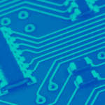

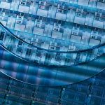
This webinar discuss about specific analysis for QC in PCB applications. It will also cover critical dimensional measurement, roughness, and defect identification.
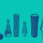
Presenters Adam Platteis and Alberto Aguerri will show solutions pertaining to ISO 4287, ISO 25178, and how Sensofar’s proprietary software quickly identifies profiles, roughness parameters, and defects for surface texture, height, and traces. The focus will be on imaging wafers, pads, step heights, bonds, and probe cards.
Sensofar solutions can be used in the R&D lab and for in-line QA/QC high-throughput environments for automatic Pass/Fail reporting. Sensofar offers standalone and customizable solutions that integrate confocal, interferometry, and focus variation technologies into a single sensor head for the semiconductor and microelectronic industries.