ADVANCED PACKAGING
Heterogeneous integration and advanced packaging are revolutionary innovations that combine different technologies into a single, compact system. This boosts performance, reduces power consumption, and enables applications with large data capacity like AI, 5G, and High-Performance Computing. They are the foundation for the future, the evolution of computing as traditional methods reach their limits.
What is heterogeneous integration?
Heterogeneous integration (HI) is a key technology that emerges from the complementarity of the two main innovation paradigms in the semiconductor industry: “More Moore” and “More than Moore.”
“More Moore” focuses on improving chip performance by scaling down transistors. By contrast, “More than Moore” recognizes that innovation is not only about making chips smaller but also about adding new functionalities.
Heterogeneous integration bridges these two approaches. It enables combining different types of chips, each specialized in a specific function, within a single package, creating compact, efficient, and highly functional systems. This is essential for applications such as IoT, artificial intelligence, autonomous vehicles, and digital healthcare, where versatile and tailored solutions are required.
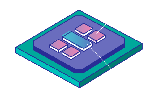
Advanced packaging solutions vary in complexity and design, offering unique advantages for improving performance, integration density, and energy efficiency.
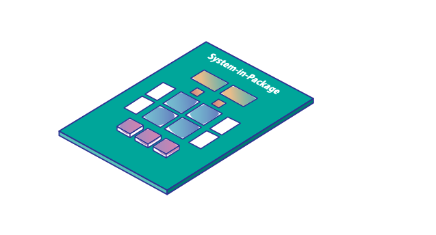
Heterogeneous integration combines materials and technologies to enhance performance, power efficiency, and scalability, as exemplified in recent developments in smart packaging sensors.

Applications
ADVANCED PACKAGING
Through-Silicon Vias (TSVs)
One key parameter to characterize these advanced semiconductor architectures is the depth of the interposer layer. TSVs are engineered to be as thin as possible to optimize space and performance in advanced packaging. The challenge lies in accurately measuring through these small but deep holes, which can be measured using the S neox and Interferometry with low numerical aperture lenses . The Hole plugin identifies and analyzes hole structures within any defined pattern.
One key parameter to characterize these advanced semiconductor architectures is the depth of the interposer layer. TSVs are engineered to be as thin as possible to optimize space and performance in advanced packaging. The challenge lies in accurately measuring through these small but deep holes, which can be measured using the S neox and Interferometry with low numerical aperture lenses . The Hole plugin identifies and analyzes hole structures within any defined pattern.
ADVANCED PACKAGING
Microbumps
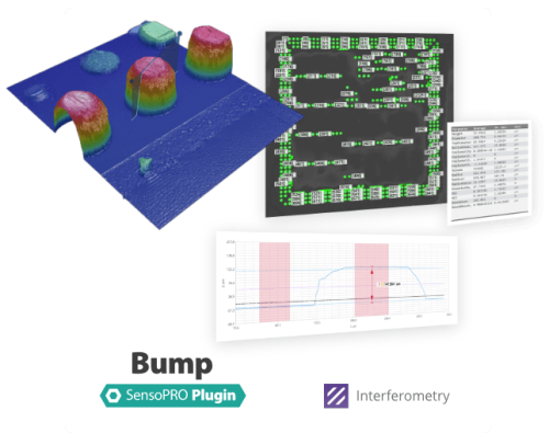
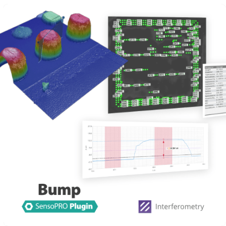
Ensure electrical and mechanical connections in stacked dies and interposers. With the S neox 3D optical profiler, we can accurately measure the height, diameter, and coplanarity to prevent bonding issues and improve performance. The Bump plugin analyzes bump structures individually or in Ball Grid Array (BGA) formats.
Ensure electrical and mechanical connections in stacked dies and interposers. With the S neox 3D optical profiler, we can accurately measure the height, diameter, and coplanarity to prevent bonding issues and improve performance. The Bump plugin analyzes bump structures individually or in Ball Grid Array (BGA) formats.
ADVANCED PACKAGING
Redistribution Layers (RDLs)
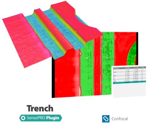
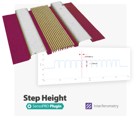
Essential for rerouting signals in advanced packaging, S neox allows the high-tech manufacturing sector to assess trace width, thickness, and surface quality to ensure signal integrity. Trench plugin can automatically detect trenches on uneven surfaces for accurate dimensional analysis.
HETEROGENEOUS INTEGRATION
Microlenses
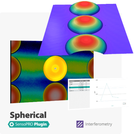
Play a key role in Photonic Integrated Circuits (PICs) co-packaged optics, imaging sensors, and AR displays, enabling advanced optical functions beyond traditional components and manufacturing techniques. The Spherical plugin analyzes spherical surfaces, extracting radius and residual roughness. Aspheric plugin analyzes surfaces using deformation coefficients and roughness data.
Play a key role in Photonic Integrated Circuits (PICs) co-packaged optics, imaging sensors, and AR displays, enabling advanced optical functions beyond traditional components and manufacturing techniques. The Spherical plugin analyzes spherical surfaces, extracting radius and residual roughness. Aspheric plugin analyzes surfaces using deformation coefficients and roughness data.
HETEROGENEOUS INTEGRATION
Co-Packaged Optics (CPO)
Integrates optical engines directly into packages, shortening links and boosting bandwidth density and energy efficiency, which are crucial for data-intensive applications such as Artificial Intelligence.
Integrates optical engines directly into packages, shortening links and boosting bandwidth density and energy efficiency, which are crucial for data-intensive applications such as Artificial Intelligence.
These approaches are pillars of advanced industrial technology and key to the HPC, 5G, automotive, and AI sectors. Sensofar helps manufacturers push the limits of performance, enabling smaller, faster, and more energy-efficient devices.
Semiconductor metrology equipment
Modern fabs need fast, flexible, and reliable semiconductor metrology tools, and Sensofar delivers just that.
Your semiconductor metrology expert
As devices grow smaller and more powerful, the need for precise and scalable metrology only grows. Whether you’re exploring the definition of wafer in semiconductor, looking for semiconductor metrology equipment, or seeking a trusted provider of metrology in the semiconductor industry, Sensofar is here to help you stay ahead.
Let’s shape the future of microelectronics, one nanometer at a time.


