Step height standards based on for 3D metrology


Step height standards based on self-assembly for 3D metrology of biological samples publication
V. Heikkinen 1, I. Kassamakov 2, T. Viitala 2, M. Järvinen 2, T. Vainikka 2, A. Nolvi 2, C. Bermúdez 3, R. Artigas 3, P. Martinez 3, V. Korpelainen 1, A. Lassila 1, and E. Hæggström 2
1 VTT MIKES, Tekniikantie 1, 02150 Espoo, Finland
2 University of Helsinki, Fabianinkatu 33 00014, Helsinki, Finland
3 Sensofar-Tech, S.L. (Spain)
Published 23 June 2020 • © 2020 IOP Publishing Ltd
Measurement Science and Technology, Volume 31, Number 9 NanoScale 2019
Abstract
Modern microscopes and profilometers such as the coherence scanning interferometer (CSI) approach sub-nm precision in height measurements. Transfer standards at all measured size scales are needed to to guarantee traceability at any scale and utilize the full potential of these instruments, but transfer standards with similar characteristics upon reflection to those of the measured samples are preferred. This is currently not the case for samples featuring dimensions of less than 10 nm and for biosamples with different optical charasteristics to silicon, silica or metals. To address the need for 3D images of biosamples with traceable dimensions, we introduce a transfer standard with dimensions guaranteed by natural selfassembly and a material that is optically similar to that in typical biosamples. We test the functionality of these transfer standards by first calibrating them using an Atomic Force Microscope (AFM) and then using them to calibrate a CSI. We investigate whether a good enough calibration accuracy can be reached to enable a useful calibration of the CSI system.
1. Introduction
Modern microscopes and profilometers, such as the coherence scanning interferometer (CSI) which is often also called the scanning white light interferometer (SWLI), approach sub-nm precision in height measurements. As they offer a larger field of view (FOV) than e.g. the atomic force microscope (AFM), which has previously been used to calibrate low steps, interferometric profilers open new measurement opportunities [1, 2]. With a large FOV, however, come limitations. The diffraction-limited horizontal resolution makes small features difficult to see clearly, and also the vertical precision for horizontally small features is degraded as their edges become blurred [3, 4].
For the CSI, accurate calibration of the vertical scale can be difficult, as this scale typically depends on the accuracy of the height encoder and the properties of translation. Depending on the kind of encoder and translator, there can be different types of non-linearities and other error sources e.g. Abbe error. The interferometric Z-scale [4, 5, 6] such as is used in a metrological AFM (MAFM) [7] is one solution, but it is costly, adds complexity and also patent issues can prevent its use. Thus, physical transfer standards (TS) are usually favoured as a method to bring traceability into CSI measurements [8, 9], but also e.g. adjustable height standards have been tested [10, 11]. In addition to translator errors, it is necessary to test the surface localization algorithm of the CSI, as this algorithm can produce errors that are independent of the scanner but dependent e.g. on the used light spectrum and surface properties. For larger step heights there are a variety of step height standards and gauge blocks to calibrate to this scale. However, for <10 nm steps it is difficult to find good TS. Thus, non-linearity in the Z-scale at nm scale could go unnoticed. This issue becomes important when the CSI is used to measure features that are only a few nm high. Noncontacting areal measurements such as those done with the CSI and typical error sources of such measurements are covered by the ISO 25178 standard especially parts 600 and – 604 [12].
Typical silicon or metal calibration standards differ optically from biosamples. They create a phase change in the light upon transmission or reflection that differs from that present when measuring biological samples. This artifact can lead to uncontrolled and a hard-to-identify offset in measured heights [13], however for a step with two similar surfaces the phase errors cancel out each other.
To address the need for undistorted 3D images, we introduce a TS the dimensions of which are guaranteed by natural self-assembly. The traceability of the TS to the SI metre can be achieved by calibrating the TS with e.g. a metrological AFM [7] or traceable interference microscope in a suitable laboratory.
Here we test a self-organized structure of height 5 nm to calibrate a CSI at nm scale. The structure should allow calibration of the vertical scale of the CSI at a precision limited by the calibrated instrument. The sharp corner features within the structure could also be useful for studying the 3D transfer function of the CSI. We measure an 8-step staircase produced using the same technology. This structure could allow testing height magnification and linearity of the CSI on a scale of 5–40 nm.
2. Transfer standards
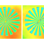
The TS are based on applying Langmuir-Blodgett films (LBF) of a certain material (e.g. stearic acid) onto a desired surface (e.g. mica or glass microscopy slide) to form a flight of steps. The nature of the LBF makes every single layer equally thick, only a few nm thick. Partly overlapping placement (horizontal offset) or overlapping the layer at a certain angle, these films produce a step structure suitable for both offline instrument calibration and for online and in-view calibration purposes (Fig. 1).
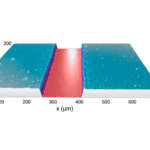
The TS were manufactured with the LBF technique in a KSV Minitrough (KSV Instruments, Helsinki, Finland). Briefly, a monolayer of stearic acid was first spread onto a subphase containing 50 μm uranylacetate and compressed at 10 mm/min to a surface pressure of 45 mN/m. Then, eight bilayers of the stearic acid monolayer were transferred onto a glass microscopy slide. This was achieved by intermittently immersing and withdrawing the slide into the subphase through the stearic acid monolayer 16 times at a speed of 2 mm/min, while keeping the surface pressure constant at 45 mN/min during the entire deposition process. The flight of steps was formed during the deposition process at the threepoint contact line between the microscope slide, air, and the monolayer covered subphase. The distance between the flights of steps in the case of NanoRuler was realized by immersing the slide to a different depth during each bilayer deposition cycle. For the NanoStar, the angle between the flight of steps was realized by immersing the slide rotated to a different angle during the deposition process.


3. Instruments
3.1 AFM
AFM measurements were done with a PSIA XE-100 using non-contact mode. Standard silicon tips (Nunano SCOUT 350R) were used in the measurements. The AFM is calibrated using step height standards calibrated against a VTT MIKES (Finnish national metrology institute) metrological AFM [7].
The measurement area was 50 × 90 μm2 and the resolution 512 × 512 pixels2. Data analysis was done with SPIP software using the histogram method [14].
3.2 CSI
The CSI used in this work was a Bruker GT-K that provides 160 × 120 μm2 images with 0.245 μm pixel size using a 20× objective and a 2× secondary lens. This setup was used for the CSI calibration with the NanoStar. For the NanoRuler measurements and to test the uniformity of NanoStar, a 0.55× secondary lens was used to provide 560 × 420 μm2 images with 0.881 μm pixel size. The lower magnification was chosen to have enough horizontal range for the staircase sample, whereas the higher magnification was chosen to allow precise alignment of the CSI data to the AFM data for the NanoStar sample. High spatial resolution is needed, as the calibration area is near the centre of the sample where the step is relatively narrow.
To avoid issues due to non-linearity of the Z-scale, all measurements were done in an area on the Z-scale with a relatively flat gain curve. The calibration measurements were done at four different heights with 2.5 μm vertical separation in order to average out the periodic error of the CSI height encoder. The encoder has 10 μm periodicity. The measurements of the staircase sample were done at the same height as for CSI calibration. The measurements were done with the “VXI” mode that uses phase information in adjacent pixels to reduce the noise level in flat areas.
4. Results
4.1 NanoStar
First, we determined how precisely the CSI could be calibrated for such low heights. The negative step of a NanoStar sample was measured 20 times using the CSI with VXI measurement mode. The sample was not moved between measurements, and the height of the CSI z-scale varied only due to drift of the equipment during the 5-minute period between the first and last measurements. The drift in the Z direction was less than 200 nm but less than 1 μm in the X and Y directions. The repeatability of the CSI was 0.38 nm, defined by standard deviation of the measured negative step heights of the measurement datasets corresponding to a standard deviation of the mean of 0.19 nm for a calibration dataset consisting of four measurements.
It should be noted that in typical μm-scale step measurements, an uncertainty of a few nm occurs with the CSI. However, at nm scales we expect that smaller measurement uncertainty could be achieved if issues such as out-of-plane error are handled correctly. On the other hand, the reflectivity of the sample and the surface quality vary slightly, which reduces the signal-to-noise ratio of CSI measurements compared to e.g. metal-coated step height samples.
The groove depth in the NanoStar sample was calibrated using the AFM to be 5.4 nm high (Fig 3).A histogram method was used to determine the step heights. The standard uncertainty for the calibration is 0.2 nm. The main uncertainty components in the AFM measurement were the calibration of the instrument, non-linearity of the scale, tilt correction, and sample uniformity. The surface roughness of the Nanostar sample is Sa = (0.25 ±0.11) nm and Sq = (0.30 ±0.15) nm. The values measured at the different areas of the NanoStar agree within the stated uncertainties. The measured height using the CSI was 5.3 nm. The calibration was done over a 50 × 45 μm2 area near the contact point of the positive and negative steps (Figs 1–4). The difference in measured step height between the instruments was 0.1 nm, which corresponds to a scale error of -0.019 at the used part of the CSI height range. A small deviation from the value set using 10 μm – 1000 μm samples was expected, as there were visible non-linearities already at the μm scale. The uncertainty of the scale error was 0.056; thus the detected error is less than the measurement repeatability.


In a test of the structure uniformity, the tilt between the base and negative step was 0.00568 nm/μm (Fig. 5). This was defined by taking histograms 5.5 μm apart at 10 positions across the negative step. The histograms were recorded over 5.5 × 270 μm2 areas placed symmetrically across the step starting 17 μm from the centre. There were additional deviations of 0.21 nm RMS on top of the tilt in areas away from the edges of the step.

The tilt of the negative step (0.00568 nm/μm) would cause an error of 0.056 nm for a typical alignment deviation of 10 μm. The non-uniformity after substracting the tilt would cause an additional uncertainty of 0.094 nm (standard error of the mean for the used measurement area) for all alignment errors of more than 5 μm. These non-uniformities would only cause a measurement uncertainty of 0.11 nm with 10 μm alignment between calibration areas. This level of alignment can be reached when using the CSI at a magnification giving a pixel size of ~1 μm and the AFM as the reference instrument. If a larger area can be used, the noise term (0.094 nm) would decrease. For a worse alignment, only the error from the tilt term (0.065 nm) would increase.
Assuming no other error sources than repeatability, sample calibration, and non-ideal sample shape, the total uncertainty of the calibration would consist of 0.2 nm due to AFM, 0.11 nm due to sample non-uniformity, and 0.19 nm due to CSI repeatability. Thus, the total uncertainty would be 0.30 nm. This is only a 0.02 nm increase compared to a perfectly flat sample. In a typical case, the increase in calibration uncertainty would be less, due to additional sampleindependent error sources such as out-of-plane error.
5. Conclusions
A biocompatible TS for nm class height measurements using optical profilometers was investigated. Based on the results, the standards were of sufficient quality for calibrating the CSI with an accuracy limited by the measurement resolution of the instrument instead of by the quality of the standard. The standards allow calibration of CSI for heights from 5 nm to 40 nm. The sharp edge of the NanoStar standard allows determining the lateral resolution of optical profilometers in a similar way to commonly used “Siemens star” samples at larger scale[16].
Acknowledgements
This project has received funding from the EMPIR programme co-financed by the Participating States and from the European Union’s Horizon 2020 research and innovation programme. (VK, VH, and AL)
References
[1] Schmit J, Reed J, Novak E and Gimzewski J K, 2008 Opt. A: Pure Appl. Opt. 10 064001
[2] Harasaki A, Schmit J, and Wyant J C 2000 Applied Optics 39 13
[3] Xie W, Lehmann P and Niehues J, 2012 Applied Optics 51 11
[4] Leach R.K., Giusca C.L., Haitjema H., Evans C., Jiang X. 2015 CIRP Annals 64, 2, 797-813
[5] Olszak A, Schmit J 2003 United States Patent US 6,624,894 B2
[6] Novak E, Schmit J, 2003 Proceedings of XVII IMEKO World Congress Metrology in the 3rd Millennium TC2 183-186
[7] Korpelainen V, Seppä J and Lassila A. 2010 Precision Engineering 34 735–744
[8] Giusca C, Leach R, Helery F and Gutauskas T, 2011 Journal of Physics: Conference Series 311 012005
[9] Haitjema H 1997 Metrologia 34 161-167
[10] Koops R 2001 Proceedings of SPIE 4401 298-304
[11] Heikkinen V, Kassamakov I, Seppä J, Paulin T, Nolvi A, Lassila A, and Hæggström E 2015 Applied Optics 54 10397
[12] ISO 25178: Geometric Product Specifications (GPS)
[13] Harasaki A, Schmit J and Wyant J C 2001 Applied Optics 40 13
[14] The Scanning Probe Image Processor (SPIP), Image Metrology, Denmark (www.imagemet.com).
[15] Seppä J, Korpelainen V, Bergstrand S, Karlsson H, Lillepea L and Lassila A, 2014 Meas. Sci. Technol. 25 044013
[16] Weckenmann A, Tan Ö, Hoffmann J, Sun Z, 2009 Meas. Sci. Technol. 20 065103