Präzisions-3D-Messtechnik für die Halbleiterfertigung
Während die Halbleiterindustrie die Grenzen der Geräteleistung und Miniaturisierung weiter ausreizt, bleibt die 3D-Messtechnik unerlässlich, um eine gleichbleibende Ergebnisse, zuverlässige Qualität und eine schnellere Markteinführung zu erzielen.
In diesem Webinar erfahren Sie, wie die optische 3D-Messtechnik die Herausforderungen sowohl in der Front-End- als auch in der Back-End-Halbleiterfertigung meistert. Sie erfahren mehr über modernste Automatisierung für die Inline-Inspektion, Best Practices für fortschrittliche Verpackungen und die Bewertung heterogener Integrationen sowie reale Anwendungen von Tests auf Wafer-Ebene bis hin zur Verifizierung von Endprodukten.
Sehen Sie sich das Webinar an, um zu erfahren, wie die Messtechniklösungen von Sensofar Ihnen helfen können, in der sich schnell entwickelnden Halbleiterlandschaft einen Schritt voraus zu sein.
SCHWERPUNKTTHEMEN
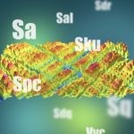
Entscheidende Rolle der 3D-Messtechnik für die Halbleiterfertigung
Verschaffen Sie sich ein klares Verständnis für die wichtigsten Herausforderungen bei den heutigen schrumpfenden Geometrien und engen Toleranzen. Erfahren Sie, wie berührungslose 3D-Oberflächenmessungen die Prozesssteuerung optimieren, Defekte reduzieren und die Ausbeute sowohl in der Front-End- als auch in der Back-End-Halbleiterproduktion steigern.
Nutzung der Automatisierung für Umgebungen mit hohem Volumen und hoher Auslastung
Erfahren Sie, wie die automatisierte Erfassung und Analyse Inspektionsschritte voranbringt, manuelle Fehler reduziert und die Entscheidungsfindung in Fabriken mit hohem Durchsatz beschleunigt. Erfahren Sie, wie integrierbare Systeme bei jedem Schritt der Halbleiterherstellung eine gleichbleibende Qualität und Wirtschaftlichkeit gewährleisten.
Chips der nächsten Generation: fortschrittliches Packaging und heterogene Integration
Lernen Sie die spezifischen Messanforderungen neuer Packaging-Technologien kennen, wie z. B. 2,5D- und 3D-Packaging, Wafer- und Panel-Level-Packaging sowie Co-Packaged-Optiken. Erfahren Sie, wie die optische 3D-Messtechnik kritische Prüfanforderungen erfüllt, um die Produktzuverlässigkeit angesichts der immer komplexer werdenden Integration zu gewährleisten.
Reale Anwendungen aus der gesamten Halbleiter-Lieferkette
Erfahren Sie, wie führende Halbleiterhersteller 3D-Messungen bei Tests auf Waferebene, bei der Inspektion nach dem Bonden und bei der Verifizierung von Endprodukten integrieren. Entdecken Sie bewährte Strategien, um Fehler frühzeitig zu erkennen, Ausschuss zu reduzieren und die Qualität in Lieferketten mit mehreren Standorten aufrechtzuerhalten.