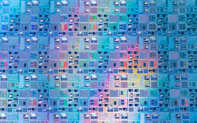
Precision 3D metrology for semiconductor manufacturing
カタルーニャ工科大学(UPC)で学士号を取得。同大学物理学部に研究アシスタントとして勤務。バルセロナ大学(UB)で修士課程を修了した後、Sensofarに入社し光学測定の世界へ入る。セールススペシャリストとして、Sensofarの光学測定に関する知識を伝播し、Sensofarのシステムの可能性を最大限に引き出す方法について顧客にトレーニングを提供している。通常はSensofarのデモルームでサンプルを測定したり、ライブデモンストレーションを実施している。
While the semiconductor industry continues to push the limits of device performance and miniaturization, 3D metrology remains essential for achieving consistent yield, reliable quality, and faster time-to-market.
In this webinar, discover how 3D optical metrology meets the challenges posed by both front-end and back-end semiconductor manufacturing. You’ll learn about cutting-edge automation for in-line inspection, best practices for advanced packaging and heterogeneous integration evaluation, and real-world applications from wafer-level testing to final device verification.
Join us to see how Sensofar’s metrology solutions can help keep you ahead in the rapidly evolving semiconductor landscape.
KEY TOPICS
Critical role of 3D metrology for semiconductor manufacturing
Gain a clear understanding of the key challenges in today’s shrinking geometries and tight tolerances. Discover how non-contact 3D surface measurements optimize process control, reduce defects, and increase yield in both front-end and back-end semiconductor production.
Leveraging Automation for High-Volume/High-Yield Environments
Learn how automated acquisition and analysis streamline inspection steps, reduce manual errors, and accelerate decision-making in high-throughput fabs. Discover how integrable systems ensure consistent quality and cost-effectiveness at every semiconductor manufacturing step.
Tackling next-gen chips: advanced packaging and heterogeneous integration
Dive into the specific metrology needs of emerging packaging technologies, like 2.5D and 3D packaging, wafer and panel-level packaging, and co-packaged optics. Understand how 3D optical metrology addresses critical inspection requirements to ensure product reliability in the face of increasingly complex integration.
Real-world Applications Across the Semiconductor Supply Chain
See how semiconductor leaders integrate 3D measurement at wafer-level testing, post-bond inspection, and final device verification. Uncover proven strategies for catching defects early, reducing scrap, and maintaining quality throughout multi-site supply chains.


