Development of confocal-based techniques for shape measurements on structured surfaces containing dissimilar materials
Development of confocal-based techniques for shape measurements on structured surfaces containing dissimilar materials full article
Cristina Cadevall1, Roger Artigas1, Ferran Laguarta1
1Universitat Politècnica de Catalunya (UPC) Rambla Sant Nebridi, 10, E-08222 Terrassa, Spain.
Proceedings Volume 5144, Optical Measurement Systems for Industrial Inspection III; (2003)
Event: Optical Metrology, 2003, Munich, Germany
Abstract
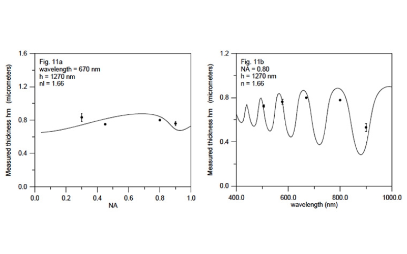
One of the applications, which is considered to be very difficult to carry out with most optical imaging profilers, is the shape and texture measurements of structured surfaces obtained from the superposition of various micro or sub-micrometric layers of dissimilar materials. Typical examples are the architectures of microelectronics samples made up of Si, SiO2, Si3N4, photoresists and metal layers. Because of the very different values of the index of refraction of the involved materials, visible light is reflected in the various interfaces. As a result, some reflected wavefronts are superposed giving rise to interference patterns, which are difficult to understand in terms of surface topography and layer thickness. In this paper we introduce a new method based on non-contact confocal techniques to measure the shape of structured samples. The method is based on the comparison of the axial responses obtained in areas of the surface where there is a layer and in other areas where there is just the substrate. To our knowledge, this approach enables the confocal profilers to measure the thickness of layers on the sub-micrometric scale for the first time.


