Semicon Taiwan
Non-contact 3D surface metrology
At Sensofar, we understand the importance of precise and reliable surface metrology in quality assurance, which is why we provide cutting-edge metrology solutions for the manufacturing industry. With Sales Offices in Asia and a global presence, we are committed to delivering innovative systems that enable our customers to improve their production processes and deliver high-quality products.
Our expertise in optical and non-contact measurement technology helps manufacturing professionals overcome even the most challenging surface measurement problems.
Discover how Sensofar can help you optimize your manufacturing processes!
The Premier Microelectronics Event
Semicon Taiwan is recognized as the leading semiconductor technology trade show in Taiwan. It brings together experts from the micro- and nanoelectronics industry from all over the world. The fair focuses on technologies used in the design and manufacturing of semiconductors, solar cells, and other micro- and nanoelectronic products, placing special emphasis on the demands of the applications market.
Visit us!

Booth
I2015

10th to 12nd
Sep 2025

Wed to Fri
9-17h

Zhubei City, Hsinchu County
Taipei
Products on the show
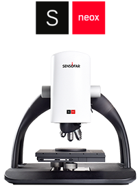
The S neox is the most versatile 3D optical system in the market. Full capabilities and measurement automation features.
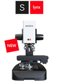
The S lynx 2 is a compact and versatile 3D optical system for roughness, volume, and critical dimensions measurements.
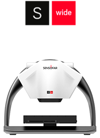
The S wide is designed to measure large areas in one shot, suited for speed and shape measurement applications.
Experience high precision
for large samples
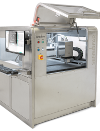
The S neox Grand Format offers a complete solution, from the hardware to the software perspective, for 3D surface measurements of large panels in semiconductor, display, and PCB industries.
Watch the webinar
Precision 3D metrology for semiconductor manufacturing
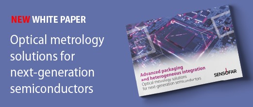
Discover how 3D optical metrology meets the challenges posed by both front-end and back-end semiconductor manufacturing. You’ll learn about cutting-edge automation for in-line inspection, best practices for advanced packaging and heterogeneous integration evaluation, and real-world applications from wafer-level testing to final device verification.


