Semiconductor and microelectronic industries overview – An interview with Alberto Aguerri

Sensofar’s VP of Sales Alberto Aguerri was recently interviewed by Adam King, editor at AZO Network about optical metrology solutions in the semiconductor and microelectronics industries.
AZO Network is an online platform with industry specific sites related with Materials Engineering, Optics, Sensors and Nanotechnology to Medical, Life Sciences and more…
Could you start by giving our readers a brief introduction to Sensofar and the company’s areas of operation?
Sensofar was founded in 2001 and has a large global footprint in Asia, Europe, and the United States. The company has around 75 employees and we have sold approximately 1,000 systems globally. These systems can be found in various industries, including semiconductors and microelectronics, aerospace and automotive applications, medical devices, and a range of scientific applications in universities.
Throughout the early part of this millennium, the company’s focus was on understanding target markets and developing technology and in 2008 Sensofar shifted to focus more on sales and strategize growth.
By 2014, we had diversified our product portfolio. We offer our flagship system, the S neox 3D Optical Profiler, alongside a range of other systems from sensor heads to motorized systems.
We have developed a number of solutions specifically aimed at the microelectronics and semiconductor industries and we have seen a great deal of growth in these two sectors, with much of the focus being on how we can improve quality in the PCB and semiconductor markets.
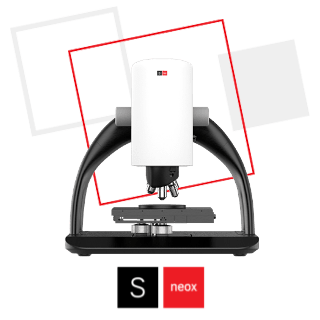
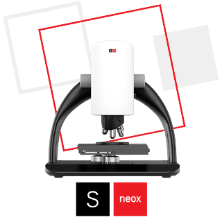
Can you give us an overview of the S neox 3D Optical Profiler?
The 5th generation of S neox 3D optical profiler is the fastest scanning confocal profilometer on the market. It is extremely easy to use and has some key advantages over previous models. We have moved to a bridge design for increased stability and the sensor head utilizes improved algorithms to produce the fastest system on the market with no moving parts and, therefore, minimum service requirements or need for extensive calibration.
“Sensofar offers unique proprietary technology and is the only company in the world to integrate confocal, interferometry and focus variation into a single sensor head. It is also possible to measure thin and thick film. Continuous confocal algorithm offers speeds about five times faster than any laser-based confocal rastering system.”
Our coherence light interferometry and phase shifting interferometry allow the S neox to achieve sub-nanometer resolution (when required). Finally, the texturization capability of our new active illumination focus variation is particularly unique, allowing us to achieve almost confocal resolution.
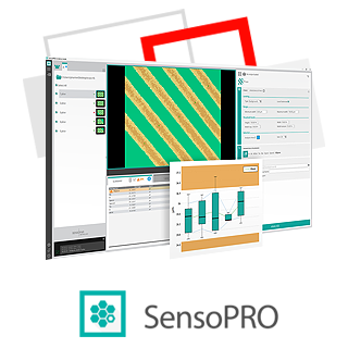
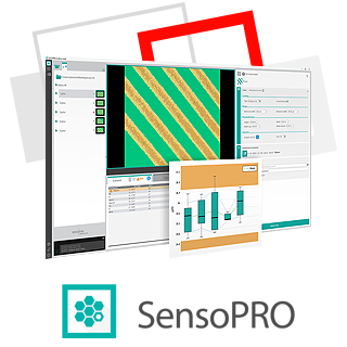
How does the SensoPRO software package work alongside the S neox 3D Optical Profiler?
Sensofar has several analysis softwares, SensoPRO is the most popular automated solution. Most systems offer the manual capability of draw measurements or deduce roughness values, but to reduce any type of subjectivity, an engineer can also create an acquisition program, which will then automatically be analyzed by the automated SensoPRO program.
“SensoPRO offers a package of different plugins that measure specific features (bumps, holes, traces…) which automatically will be detected, analyzed and reported. This is common practice when measuring large batches or when working with many of the same types of samples where it is important to ensure that no parameters have changed between measurements.”
Since the S neox brings into the table automatic measurements once established the acquisition recipe, joining the S neox with SensoPRO results into automatic acquisition and analysis. You click Acquire in SensoSCAN and you get a pass and fail report.
What sort of measurement capabilities are typically required in the semiconductor and microelectronics industries?
We are talking about two industries that have high “expectations”/requirements on their products. The most popular technologies for surface characterization are Confocal and Interferometry, since they exhibit the best lateral and best vertical resolution, respectively.
To provide one example, in wafer assembly, the front-end is typically how the wafer is manufactured and the back-end deals with the wire bonding and the packaging. Sensofar’s main strength is in the back-end.
Chips are commonly cut with diamond that normally perform two separate cuts. The first cut is to separate, and the second cut is to be a smaller measurement to ensure that there is no damage to the chip. These cuts can have a wide range of sizes and having a microscope that has different technologies is extremely convenient since the ideal technology can be selected per each size.
These dual-step heights can be measured manually, or they can be measured automatically through SensoPRO. There is a range of other key measurement parameters, all of which can be accommodated by the S neox and SensoPRO.
What sort of measurements are important in quality control applications and how does Sensofar work with customers to implement these?
To start with, dimensional analysis is one of the main checks: MEM industries have a need of measuring the radius across a flat area, radius that with lower-powered microscopes cannot be captured. Also, traces in CSP back ends are easily imaged with confocal or interferometry technologies with 0.5% repeatability error.
In PCBs characterization though, roughness is essential to understand adhesive properties of the PCB. You can either manually have those calculations or program SensoPRO to automatically provide that data for you. SensoPRO can calculate any roughness parameter defined by the areal standard ISO 25178.
For this measurement, there’s people using a Stylus profiler, which is not only destructive but also provides very limited information. Understanding the surface as an area and using Sa areal parameter will definitely give a better insight of the sample. For those people that use stylus and want to do the big jump to areal, we do have the ability to correlate Ra with Sa.

Another recurrent application is in CMP machines. Using the S neox, lifecycle’s stage of their pads can be known. Typically, vendor will ensure 8h of lifetime. Measuring with the S neox using a water immersion objective, the pads can be measured all the time and, thus, its state can be corroborated. This practice has led to use the pads between 28-30h, resulting in an important cost saving function.
For photovoltaics or solar cells, measuring the real 3D surface area allows us to understand the efficiency of the solar cell. SDR is an ISO 25178 parameter that allows us to understand how much surface area is actually collecting light. This parameter gives the total area of the topography, as if we were stretching it and measuring the 2D area that it would occupy.
What strategy does Sensofar follow to measure large batch of samples?
The SensoSCAN software can automatically prompt the microscope to recognize where the fiducial markings are on a sample and then move to the areas of interest for the actual measurement. Fiducials represent a way to load different samples and make sure that all the established positions in the acquisition recipe will be correctly measured.
This approach is useful for a multi-user lab, for example, where the engineer that creates the routine would be the only individual that would have control over any potential changes. That’s why SensoSCAN, the acquisition software, has 3 levels of operation: Administrator, Advanced Operator and Operator.
Do you characterize defects in the semiconductor and microelectronics industries?
For defect mode analysis, we generally look at a bond pad defect. These are probe depths, and it is important to understand how close that impression came to the underlying chips.
We see this often in the cell phone industry, where if the impression is too close, it could cause a failure. While it may be easier to buy a new phone if this happens, we also see these chips in use in the automotive industry, where failure could be the difference between a car stopping or not stopping.
It is important to ensure that these chips do not fail, and we can measure this with a single field of view relatively quickly. This can be done using our interferometer and we can determine the depth of the bond pad impression. Effective wire bonding requires an understanding of force. If the force is too weak, there is potential for the bond to separate, but if it is too strong, it could create cracks or damage the underlying layers.
Sensofar’s solutions include the capability to measure an image with a 10x interferometer lens. Competition does not always offer that capability, so in order to achieve this resolution, they would acquire a 50x or a 100x measurement of the same field of view in confocal, then stitch together multiple X and Y images to creating a mosaic. This is time-consuming and it does not offer the same vertical resolution as an interferometer.
What methods and techniques should be considered when working with wafers made from silicon and other materials?
When working with Gallium Arsenide (GaAs) wafers, it is important to be aware of the amount of VIAs (electrical paths) and the dimensions of these. Here SensoPRO is key since it includes a plugin that allows users to automatically determine VIAs’ bottom or top diameter, height and relative X-Y position to one another.
Roundness of the VIA is also a critical dimension and SensoPRO gives a detailed description: top and bottom diameter, height, X position of the hole and distance between the center of the top and the bottom circle. This plugin comes with different parameters to adapt to the measurement. All our plugins are configurable, we can add and remove parameters to suit better the sample to measure.
Other features typically characterized in wafers are trenches, traces, step heights or laser engravings. We offer the two solutions: manual measurement of them, where a report can be customized to the way that the quantitative and qualitative information is presented; and the automatic approach which comes in hand with SensoPRO, having a specific plugin for each feature. The result is accurate measurements within a pass and fail report.
“In Sensofar, we have always been open to custom generation of plugins and, actually, all 30 plugins that can be found in SensoPRO have come out of an inside development to solve our client’s needs.”
Understanding warpage is also highly important and Sensofar can achieve this through the coordinate function routine. There is no need to measure the entire wafer, although the system can handle wafers that are six inches or larger.
Instead, we can measure 21 predetermined points in around 2 minutes and 45 seconds, achievable at 20x with our confocal capability. This approach does not require any stitching but still gives us 0.5 micron or 500 nanometer resolution, which is enough to understand the warpage or the bow of a wafer.
Finally, can you give our readers a brief summary of Sensofar’s unique approach and capabilities?
Sensofar offers the fastest scanning confocal microscope in the market, allowing users to save time and money in any of their work, analysis, or research. We also offer the most versatile scanning profiler on the market, being the only company in the world to offer confocal, interferometry and focus variation all in one sensor head.
SensoPRO is born out of custom plugins generated for our customers, and right now constitutes a software package offers a fully automated solution for the QC market.
Sensofar offers the possibility to perform freehand measurements with the default analysis software SensoVIEW, but many of our customers in the microelectronics and semiconductor industries employ the SensoPRO’s automation capabilities to eliminate any subjectivity in their analysis routines.
Sensofar welcomes the opportunity to accommodate customer needs. We are flexible and able to provide custom solutions, even for challenging samples or applications.
To learn more about the system and software that Mr. Alberto Aguerri has been introducing click on the following images: